


Laser Decap Machine: It is suitable for semiconductor chip failure analysis to remove the surface molding compound of the chip by laser, so as to observe the internal failure point.
|
Equipment Size |
800x600x1500mm |
Repeat Accuracy |
±0.03m |
|
Laser Power |
20W |
Power Supply |
AC 220V, 10A |
|
Laser Wavelength |
1064nm |
Source Gas |
CDA |
Product Feature And Application
- Proprietary software algorithm, no damage to the base material.
- After laser decap, only one drop of acid can achieve decapping.
- The support of the power chip can be dissolved to expose its lower wafer.
- It can dissolve all kinds of solder of power MOS to prevent solder from blocking wafer.
- Provides kinds of decapping potion formula.
- The PI layer covered on the IC can be effectively dissolved to prevent the PI layer from affecting the microscopic observation.
- The IC wire can be maintained, convenient for subsequent failure analysis.
- With a visual function, the chip can be operated under the camera, easy observation.
Production Details

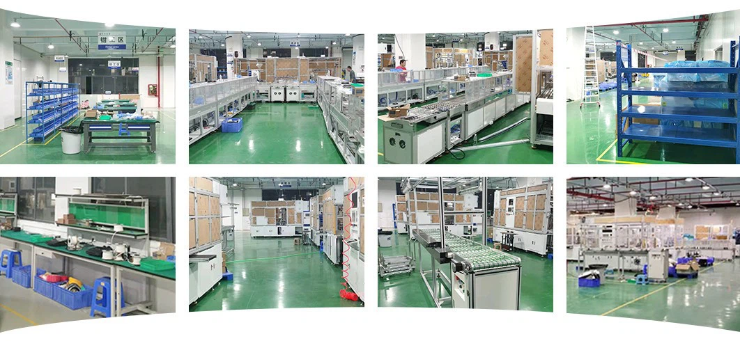
Our Factory And Workshop

Certificate

Cooperative Partner

FAQ
Q: What is a laser decap machine?
A: Laser decap machine is a kind of equipment that uses laser to remove the molding compound on the surface of the chip and facilitate the observation of the internal failure point.
Q: Which products is the laser decap machine suitable for?
A: Applicable to various package types of chips.
Q: Is there anything else you need to do after the laser is off?
A: A drop of acid is needed to dissolve a thin layer of plastic sealant on the chip.
Hot Tags: semiconductor laser decap machine, China semiconductor laser decap machine factory, De cap machine, laser de cap machine, Fiber laser Decapsulation equipment, fiber laser decap machine, Semiconductor Laser Decap Machine, laser open cap machines


