

Semiconductor Transfer Machine
Chengdu Huazhuo Semi-Equipment Co., Limited specializes in providing customized and standard equipment, production line inspection and testing equipment, as well as laboratory reliability testing and failure analysis instruments for the semiconductor chip manufacturing, packaging, and testing industries.
-
![Wafer Sorter]()
-
![Semiconductor Chip Packing Line]() Semiconductor Chip Packing LineSuitable for pre-shipment packaging of semiconductor chips, applicable for inner packaging and outer packaging processes of products such as tray carriers, reel carriers, etc.read more
-
![Chip Pick & Place Aoi Machine]() Chip Pick & Place Aoi MachineIt is mainly applied to transfer between chip carriers after saw and do AOI.read more


Why Choose Us
Our Factory
We has dozens of R&D personnel and more than 500 square meters of office space.Production base: Factory area: 3600㎡ (Shenzhen) +1000㎡ (Chengdu), the number of employees: more than 120 people.
Our Service
Offer comprehensive product information, technical specifications, and insights into packaging, testing, and factory construction. Develop customized solutions in response to the unique requirements of each client.
Professional Team
The company integrates independent research and development, design, manufacturing, and after-sales service. Leveraging a team of seasoned professionals in semiconductor chip manufacturing and packaging equipment processes, the company continuously innovates and optimizes its products and services.
Production Market
Our equipment has successfully passed the ISO9000 quality certification, with annual sales reaching 150 million in the Greater China region. Additionally, our products are exported to countries such as Singapore, India, Thailand, Mexico, Malaysia, and Vietnam.
Types of Semiconductor Transfer Machine
We offer the following Product introduce:
Wafer Sorter
It is mainly used for the transfer of wafers between carriers.
A variety of loading and unloading methods can be selected.
Suitable for a variety of wafers
Can be used for transfer between various vehicles
Can be used on TAIKO wafers and normal wafers
Semiconductor Chip Packing Line
Suitable for pre-shipment packaging of semiconductor chips, applicable for inner packaging and outer packaging processes of products such as tray carriers, reel carriers, etc.
Integrated design saves labor
Manual and automatic combination, applicable to a variety of packaging specifications.
Each process scan code, information comparison, to prevent mixing.
Chip Pick & Place Aoi Machine
It is mainly applied to transfer between chip carriers after saw and do AOI.
A variety of loading and unloading methods can be selected.
Translation type and turret type are available.
High accuracy, high UPH.
With AOI function, the chip can be inspected on all six sides.

We offer the following Product Specifications:
|
Wafer Sorter |
|
|
Work |
Semiconductor substrate |
|
Work Size |
300mm |
|
Work Thickness |
600-850μm |
|
Power Supply |
AC200V, 15A |
|
Cassette (container) |
FOUP・FOSB・OPEN・PFA |
|
Throughput |
25 sheets/1 cassette transfer time 300 seconds or less |
|
Drive System |
Motor drive (servo) |
|
Equipment Weight |
About 500kg |
|
Equipment Size |
W1000 × D1400 × H1800 (mm) |
|
Transportation Unit |
1 unit・5 units・25 units |
|
Safety Mechanism |
Presence of cassette, presence of wafer, overload detection, error alarm, emergency stop |
|
Option |
Static eliminator (ionizer), full cover, area sensor ID reader, alignment, wafer flipping, etc. |
|
Model |
ALC |
Aoi Machine |
|
PCB Specifications |
||
|
Max. PCB size (X x Y) |
510mm x 460mm |
(Double lane) :510mm x 330mm |
|
Min. PCB size (Y x X) |
50mm x 50mm |
50mm x 50mm |
|
PCB Thickness |
0.6mm-6mm |
|
|
Board Edge Gap |
Top: 3mm Bottom: 3mm (Width of transport belt contact with PCB/fixture) |
|
|
Max. Bottom Gap |
50mm |
|
|
Max. Top Gap |
35mm |
|
|
Delivery Speed |
1500mm/s (MAX) |
|
|
Transmission height from the ground |
900±30mm |
|
|
Transmission lane direction |
Left-Right,Right-Left,Left-Left,Right-Right |
|
|
Transmission method |
One Stage lane |
|
|
PCB clamping method |
Edge locking substrate clamping |
|
|
Image parameters |
||
|
Camera |
GigE Vision (Gigabit network interface), Resolution: 2448 x 2048(5 Mega Pixels) |
|
|
FOV |
36mm x 30mm |
|
|
Resolution |
15 μm |
|
|
Lighting System |
Multi-angle surrounding LED light source |
|
|
Performance Parameyers |
||
|
Inspecting Contents |
Missing parts, misalignment, tilted feet, virtual soldering, offset, pole reversal, tombstone,bridging, less tin, floating pins, bent pins, etc |
|
|
Equipment |
||
|
Power requirements |
AC220V±10%,50/60HZ,1.8kVA |
|
|
Compressed air requirements |
4~6Kg/cm2 |
|
|
Operating system |
Windows 10 |
|
|
External dimension |
1090mm(L) x 1290mm(W) x 1534mm(H)(Without light,monitor and keyboard) |
L(1090mm) x W(1500mm) x H(1534mm),(without tri-color lights, monitor and keyboard) |
|
Machine weight |
About 750KG |
About 850KG |
|
Environment temperature |
4~40˚C |
|
|
Absolute humidity |
25-80%RH4 |
|
|
Communication Method |
Standard SMEMA Connection |
|
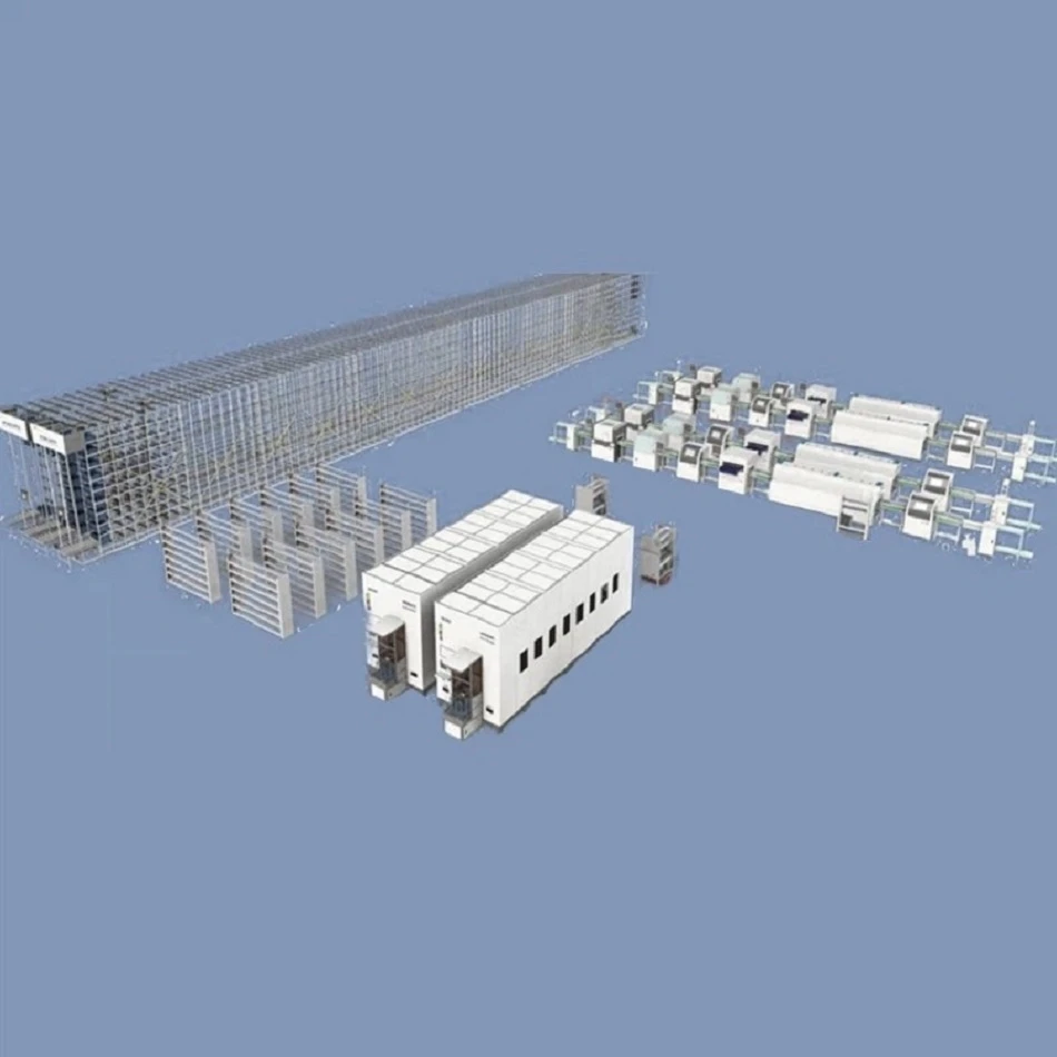
The first step in the semiconductor manufacturing process is creating silicon wafers. These wafers are what everything will be built on and need to be incredibly smooth and have few defects. The most common way to create these wafers is called the Czochralski Process. In this method, a small seed crystal of silicon is dipped into a molten pool of silicon. The crystal is slowly pulled out and rotated so that a large boule or cylindrical ingot of single-crystal silicon forms. Once the ingot has cooled, it's cut into thin disks or wafers.
Now that the wafers have been created, they need to have circuitry patterns printed on them. This process is called photolithography and uses light to print the desired pattern onto the wafer.
First, the wafer is coated with a light-sensitive material called photoresist. Then, a mask (which is basically a stencil of the desired pattern) is placed over the wafer and both are exposed to ultraviolet light. The photoresist that isn't blocked by the mask becomes harder while the exposed photoresist becomes softer. Next, the mask is removed and the now-hardened photoresist acts as an etch-resistant barrier during the next step in the process.
Once the circuitry patterns have been printed onto the wafer, it's time to start building up layers of materials on top of it using chemical vapour deposition (CVD). CVD creates a film of material on top of the wafer by breaking down gases and depositing their molecules onto its surface in a very controlled environment. This allows for highly consistent films with few defects to be created. After each layer has been deposited, more photolithography takes place to pattern each new layer until all of the necessary layers have been built up.
The final step in this process is called etching where unwanted material is removed from between the different layers using either wet chemical etching or plasma etching. Wet chemical etching uses strong acids or bases whereas plasma etching uses ionised gas—or plasma—to remove material.
Once all of the unwanted material has been etched away, you're left with your finished product: a completed semiconductor chip ready to be used in all sorts of electronic devices!
Packing & Delivery
The machine packing
Usually use the PE foam package
The base need wood package
The tape will fixed the machine on the container
The machine package arrange
The machine will arrange the drawing of each machine on the container before loading
Save the space for our client
Ensure the machine delivery 100% safty
Certificate

FAQ
We're well-known as one of the leading semiconductor transfer machine enterprises in China. If you're going to buy high quality semiconductor transfer machine, welcome to get free sample from our factory. Also, customized service is available.